Applications
- Architectural glass
- Touch screens and flat monitors
- OLED applications
- Smart-glass applications
- Transparent antistatic foils
- Photovoltaic cells
- De-icing and heating applications
- Batteries
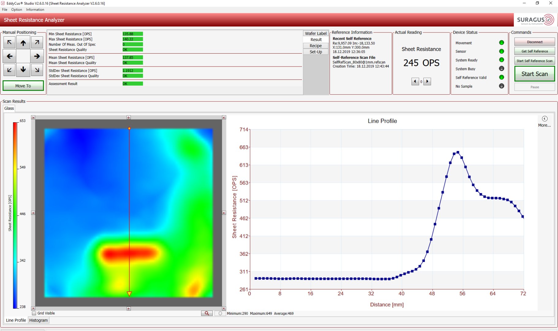
EddyCus® TF map 2525SR/5050SR i是特別設計,為在玻璃、晶圓,塑膠或箔片上的導電薄膜的測量系統,為單點非接觸式的方法, 即時測量薄厚和片電阻值。這台儀器提供導電薄膜正確又快速的高空間解析度mapping和金屬膜厚的監測 。這台非接觸的mapping 功能,能有利於對以下的製程做品質驗證:
| 透明薄膜 | 金屬薄膜 |
|---|---|
| Carbon Nano Tubes and Nano Buds | Aluminum |
| Graphene Films | Molybdenum |
| Metal Nano Wires | Silver |
| Nano Particle Films | Copper |
| and many more | and many more |
這款片電阻分析儀器具有非常人性化的圖像介面設計和數據預覽。製程測量的結果也可以選擇用圖像分析來表示。 另外,柱狀圖和軟體分析工具也都內建在此軟體中。
EddyCus® TF map 2525SR/5050SR 是特別設計為在玻璃、晶圓、塑膠或箔片上的導電薄膜快速mapping的系統,有效使用非接觸式測量方法,可以解決以下不同的需求:
| EddyCus® TF map 2525 SR | EddyCus® TF map 5050 SR | |
|---|---|---|
| Sheet Resistance Measurement | Yes | |
| Thickness Measurement | Yes | |
| Optical Transmission | Optional | |
| Anisotropy Determination | Optional | |
| Sheet Resistance & Metal Thickness Measurement | Non-Contact Eddy Current Sensor | |
| Substrate Thickness Measurement | Ultrasonic Sensor | |
| Max. Scanning Area | 10 inch / 254 x 254 mm | 20 inch / 508 x 508 mm |
| Max. Sample Thickness (defines distances) |
2 / 5 / 10 / 14 mm (Defined by the thickest sample/application) |
|
| Sheet Resistance Range | 0.001 – 10 Ohm/sq; <2 % accuracy 10 – 100 Ohm/sq; < 3 % accuracy 100 – 1,000 Ohm/sq; < 5 % accuracy |
|
| Thickness Mapping of Metal Films (e.g. copper) | 2 nm - 2mm (in accordance with sheet resistance) |
|
| Scanning Time @ 1 - 10 mm Measurement Pitch | 4 inch / 100 x 100 mm in 0.5 to 5 minutes 8 inch / 200 x 200 mm in 1.5 to 15 minutes |
8 inch / 200 x 200 mm in 1.5 to 15 minutes 12 inch / 300 x 300 mm in 3 to 30 minutes |
| Scanning Pitch | 1 / 2 / 5 / 10 mm (other on request) | |
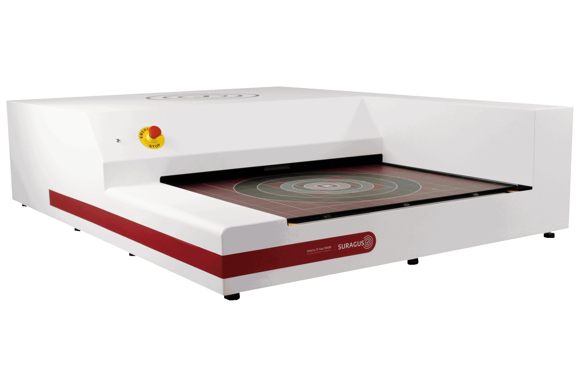
| Device Sizes (h/w/d) | 230 / 600 / 800 mm | 290 / 1180 / 900 mm |
| Weight | 27.0 kg | 120.0 kg |
| Available Features | Metal thickness tester Anisotropy sheet resistance sensor Optical transmission sensors at 632 nm wavelength |
|
REQUEST QUOTE